
Last year at InnoLAE, our Director of Revenue, Katarina Ilić, presented Voltera’s work on printing gold ECG electrodes. Building on the many engaging discussions that carried over from InnoLAE 2025, we’re excited to share that on 18 February 2026, Katarina will be presenting on direct ink writing technology for research in large area electronics. In electronics R&D, two additive technologies often come up for comparison: direct ink writing (DIW) and inkjet printing. Both are digital, maskless, and fast to iterate. But when it comes to serious prototyping and applied research, they are not equal tools. If your goal is not just to pattern materials, but to validate materials, create high-performance circuits, and de-risk manufacturing, a DIW platform like NOVA is the more powerful approach.
How direct ink writing works
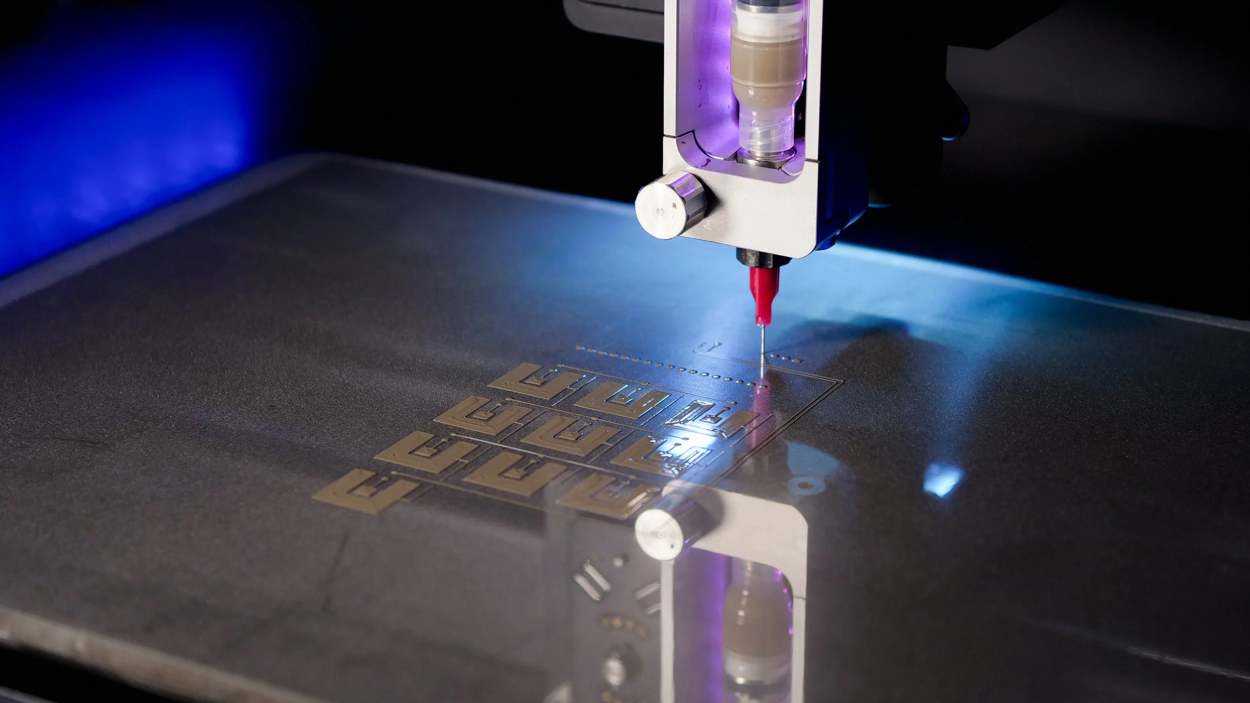
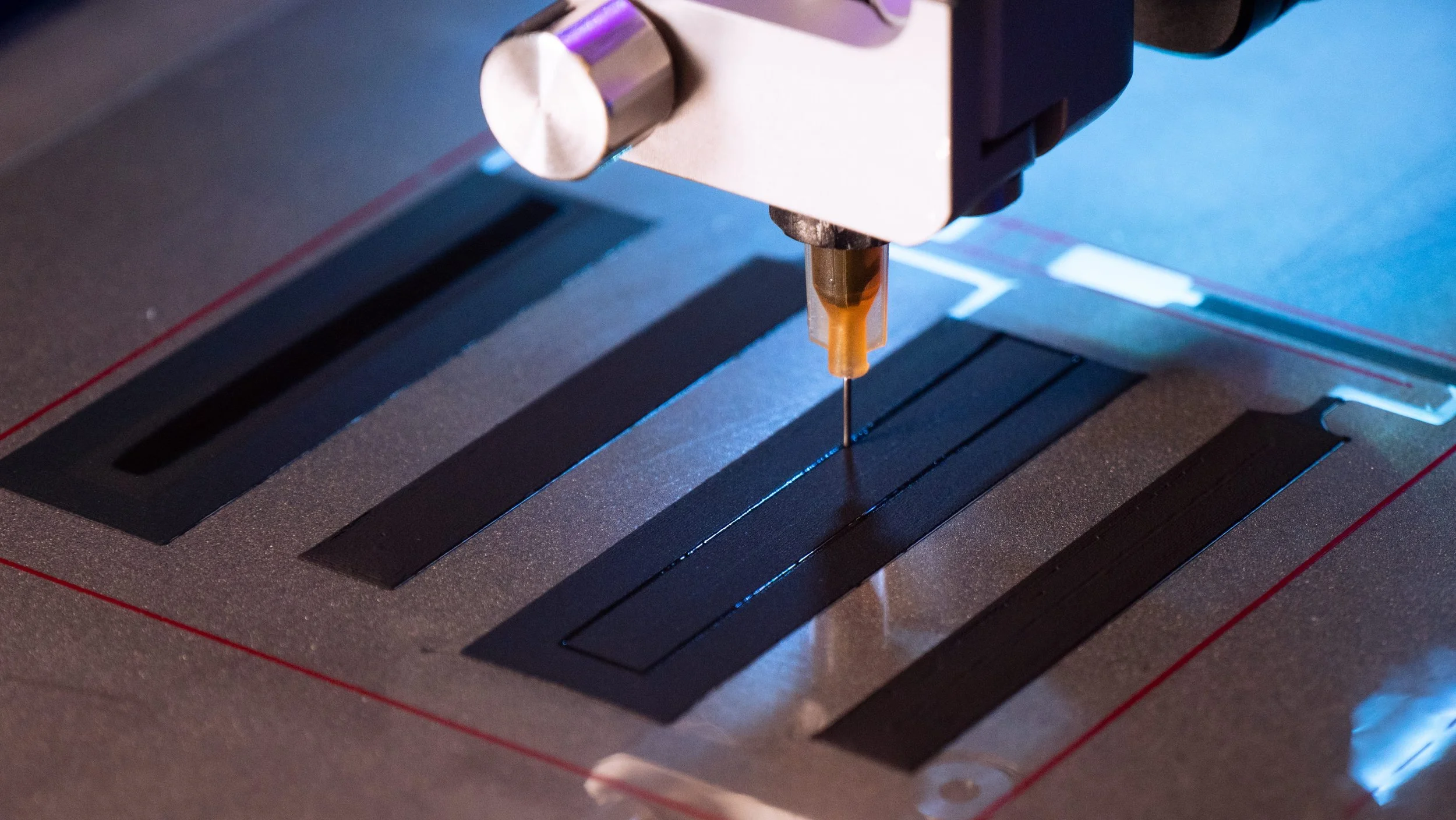
DIW is a digitally driven extrusion process where a precision syringe deposits high-viscosity conductive inks and functional materials layer by layer, following a programmed toolpath. The dispensing unit may use pneumatic pressure, a piston, or a screw-driven system. DIW supports a broad range of materials, from metal-rich pastes and polymers to ceramics and composite inks [1].
How inkjet works
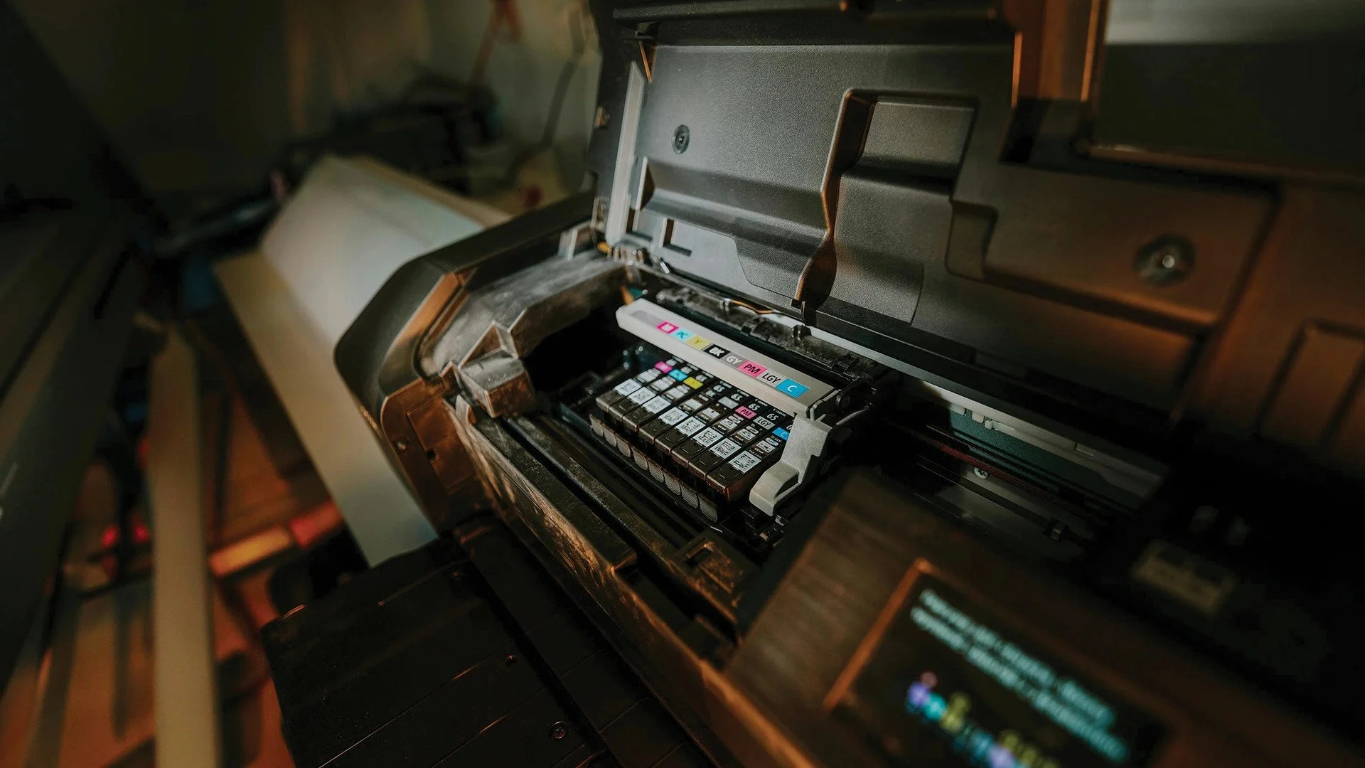
Inkjet systems eject tiny droplets (typically 0.5-100 pL) of low-viscosity nanoparticle inks via their nozzles, typically driven by piezoelectric actuators. The technology offers ultra-fine resolution, but inks must meet stringent formulation rules: low viscosity (<30 cP), surface tension ~28-42 dynes/cm, and chemically stable particle suspensions.
Key differences between direct ink writing and inkjet
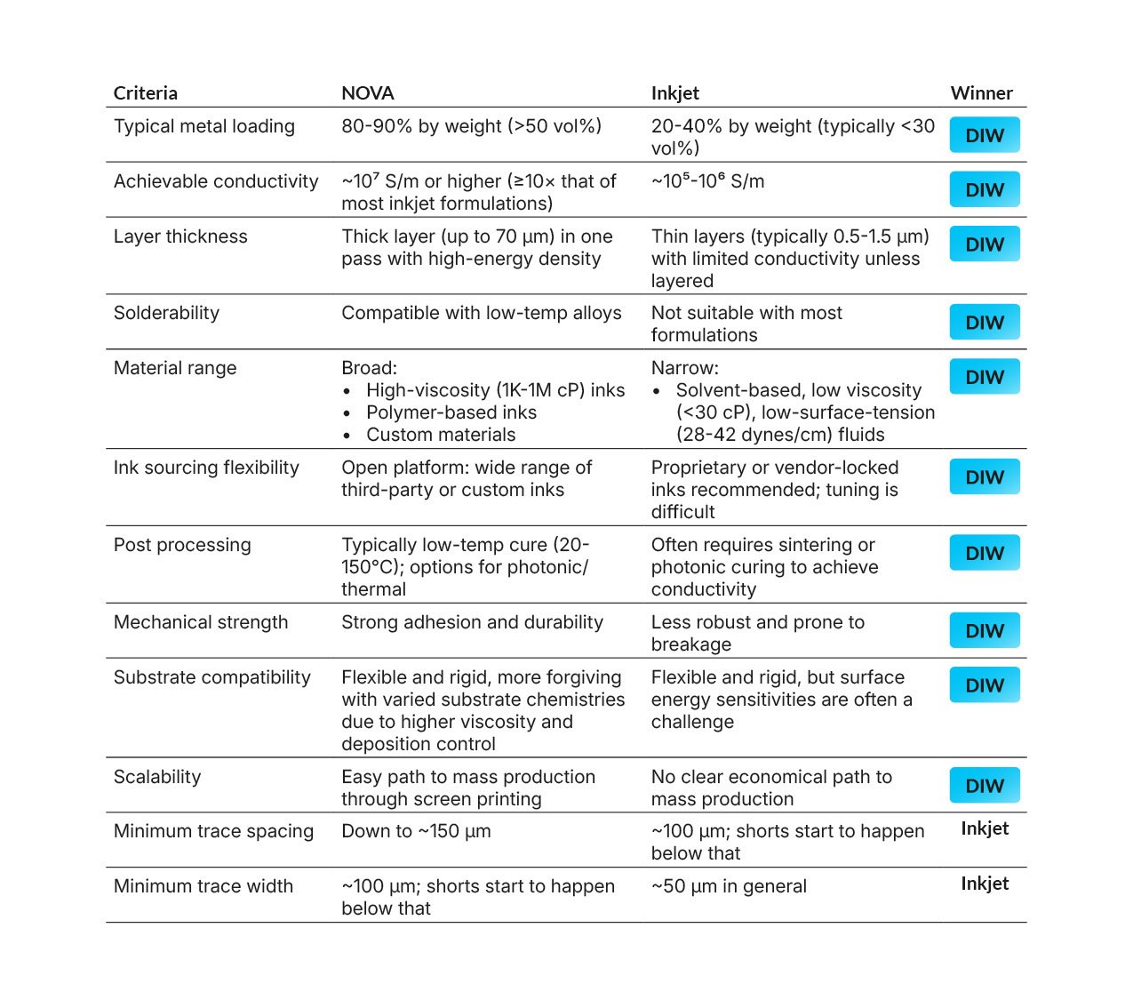
When to choose direct ink writing
As the table shows, DIW is the better fit when functional performance and manufacturability are priorities:
DIW handles screen-printable conductive pastes with 80-90 wt% metal loading, achieving ~10⁷ S/m conductivity, orders of magnitude higher than typical inkjet prints.
DIW systems work with standard solder pastes (T4, T5), enabling easy attachment of integrated circuits (ICs) and passive components.
DIW works equally well on FR1, FR4, ceramics, PET, TPU, or paper, even on fully recyclable boards.
DIW machines generally have an open ink ecosystem — researchers can experiment with custom formulations without having to source them from proprietary suppliers.
DIW prototypes made with screen-printable materials can scale easily into mass
production via established screen-printing processes.
In practice, DIW systems excel in prototyping wearables, printed sensors, soft robotics, organ-on-chip devices, and other flexible hybrid electronics [2]. These applications benefit from thicker, robust layers with larger amounts of functional material per footprint area [3] compared to inkjet.
For example, a review [1] demonstrated the use of DIW technology in printing:
Soft sensors with stable and repeatable performance, such as glove-type strain sensors with 10 integrated gauges, fabricated in under 15 minutes
High-resolution pressure sensors (100 μm features, 0.3 kPa⁻¹ sensitivity, 0-500 kPa range) by tuning rheology for 50 μm nozzles
Wearable optical and mechanochromic devices, including photonic hydrogel-based strain sensors with reversible color changes under strain
Fully 3D-printed optoelectronic and electronic components, such as QDLEDs, organic electrochemical transistors, and triboelectric nanogenerators, showing high transconductance, low operating voltage, and robustness
Printed antennas and gas sensors with porous metal microparticle arrays and tunable resonant frequencies for wireless and environmental sensing.
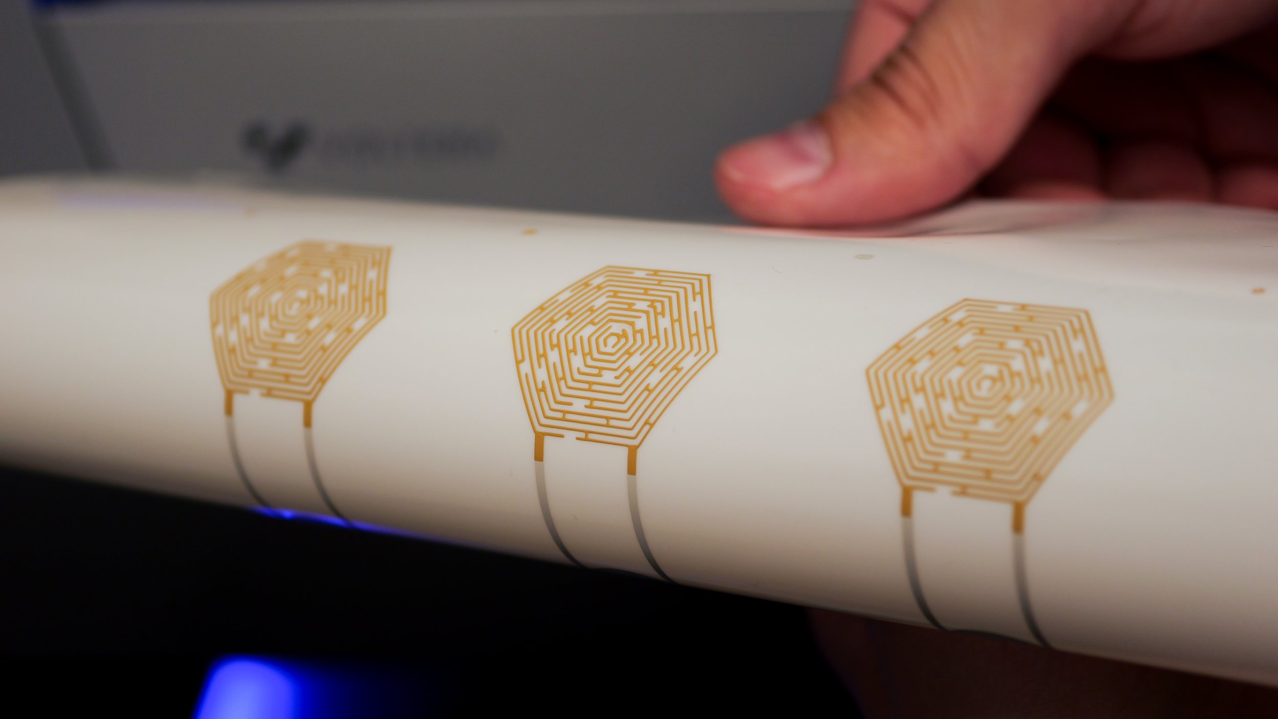
Outside of academia, industry innovators like Voltera have also been printing additive electronics and validating new materials:
When to choose inkjet
Inkjet printing is the preferred option when:
Conductivity and layer thickness requirements are modest, such as low-power, low-speed radio frequency identification (RFID) tags or disposable sensors
Ultra-fine feature resolution (<50 μm), such as for printed thin-film transistors, antenna arrays, or fine sensors
Low-viscosity materials are required, such as organic semiconductors or aqueous nanoparticle inks
Low volume R&D projects where production scalability is not a concern
In summary, inkjet is ideal when you need high-resolution patterning with low-viscosity inks and material economy in early-stage prototyping, especially where manufacturability, solderability, and mechanical durability are not the immediate concern.
Conclusion
With platforms like NOVA, DIW enables researchers to:
Publish with manufacturing-ready data while showing investors a path to mass production
Print high-performance circuits with superior conductivity, solderability, and flexibility
Handle high-viscosity, metal-rich, and custom inks
Prototype with ease — fewer clogs and lower lifetime consumable costs
That is why, for most applied research and prototyping in printed electronics, DIW is not just an alternative to inkjet; it is the more effective strategy. Interested to learn more about using NOVA for large area electronics research? Book a meeting with one of our technical representatives.
References
[1] Hou, Z., Lu, H., Li, Y., Yang, L., & Gao, Y. (2021). Direct Ink Writing of Materials for Electronics-Related Applications: A Mini Review. Frontiers in Materials, 8.
https://doi.org/10.3389/fmats.2021.647229.
[2] Hossein Baniasadi, Roozbeh Abidnejad, Fazeli, M., Juha Lipponen, Niskanen, J., Eero Kontturi, Jukka Seppälä, & Rojas, O. J. (2024). Innovations in hydrogel-based manufacturing: A comprehensive review of direct ink writing technique for biomedical applications. Advances in Colloid and Interface Science, 324, 103095–103095.
https://doi.org/10.1016/j.cis.2024.103095.
[3] Tagliaferri, S., Panagiotopoulos, A., & Mattevi, C. (2020). Direct ink writing of energy materials. Materials Advances.
https://doi.org/10.1039/d0ma00753f.