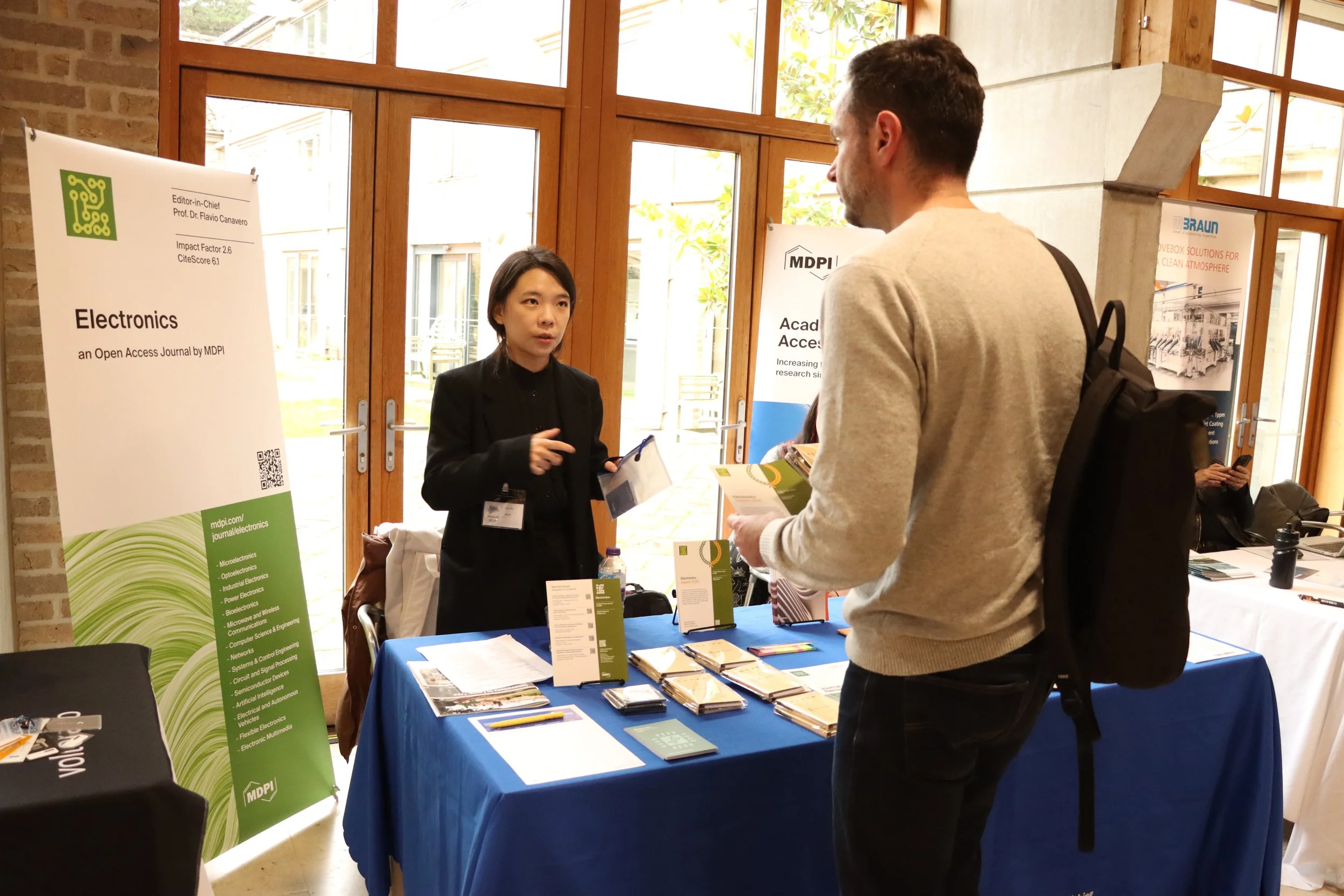
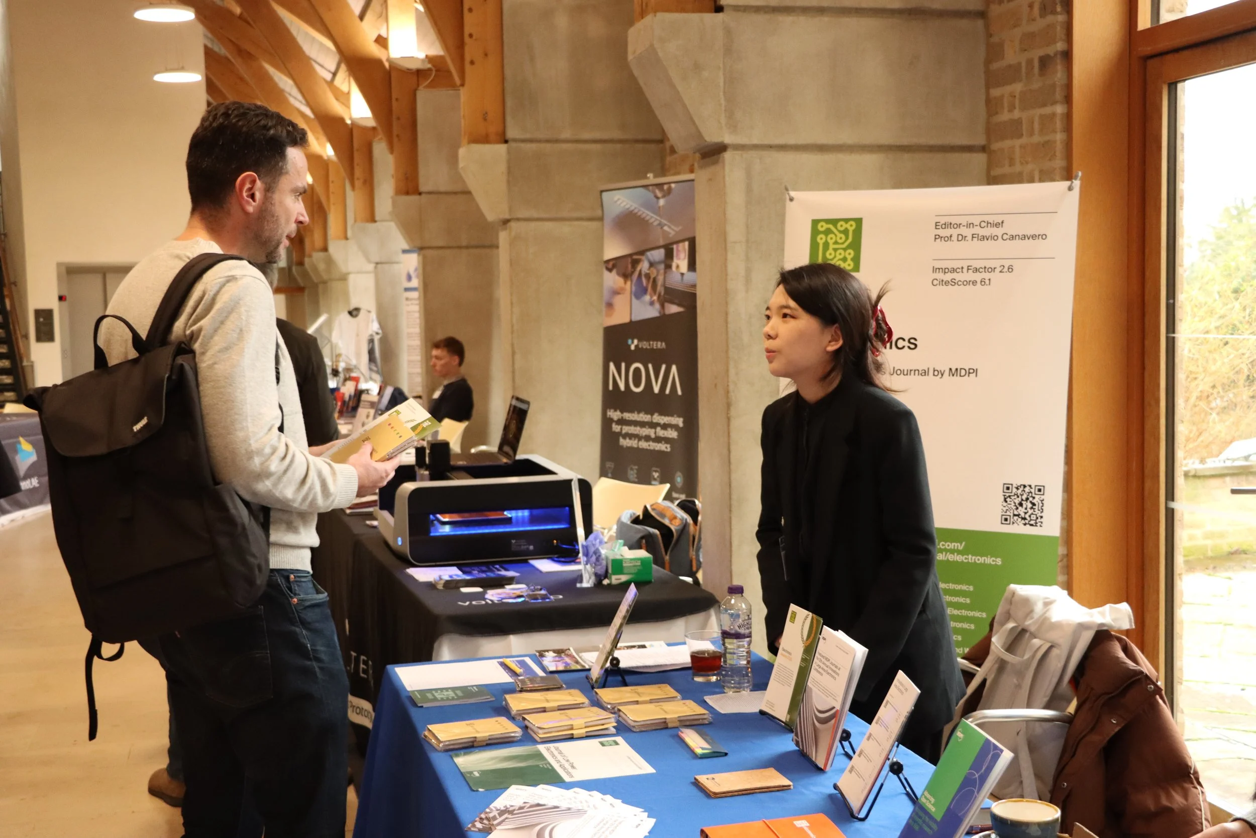
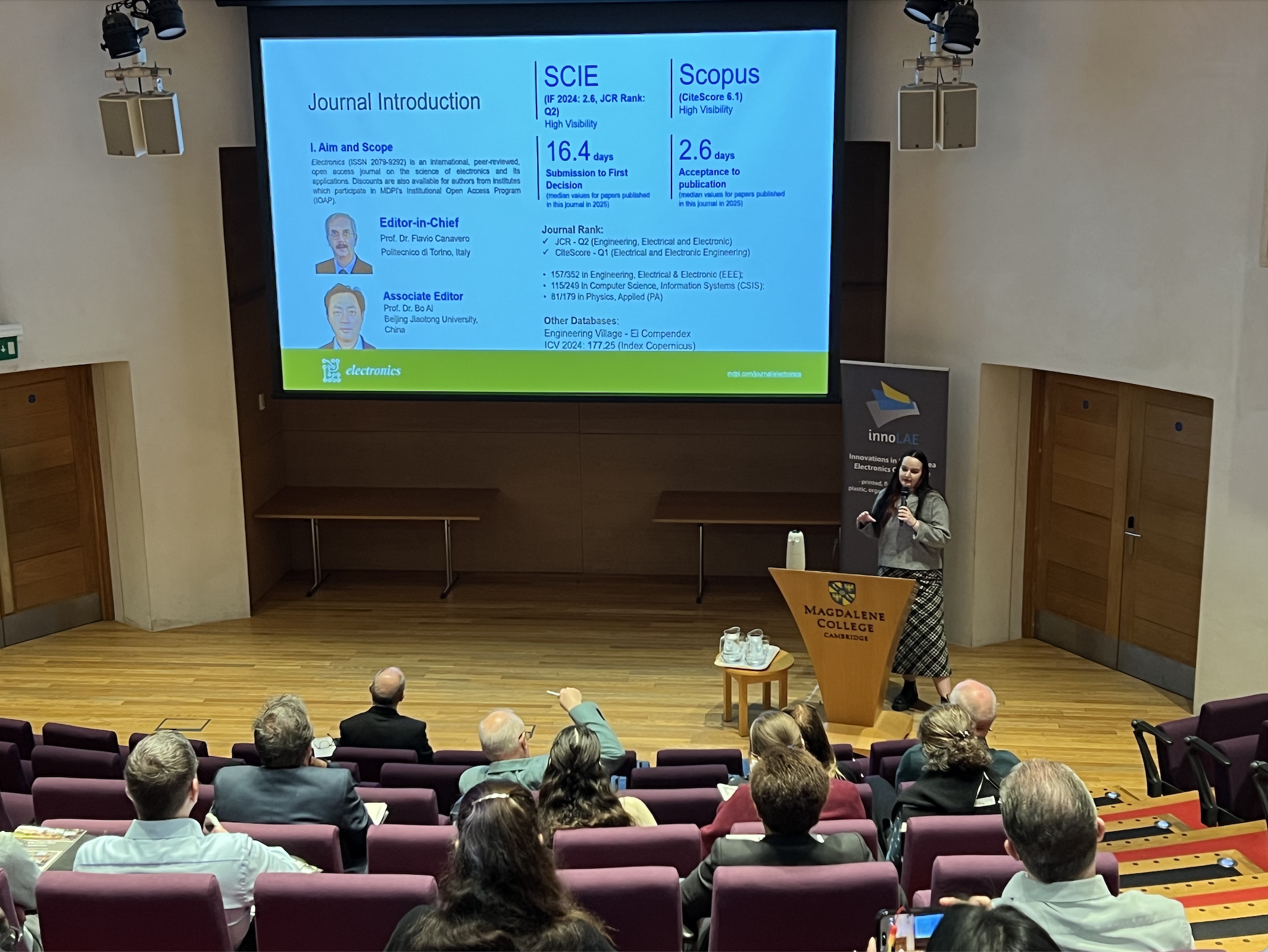
Electronics is a multidisciplinary journal designed to appeal to a diverse audience of research scientists, practitioners, and developers in academia and industry.
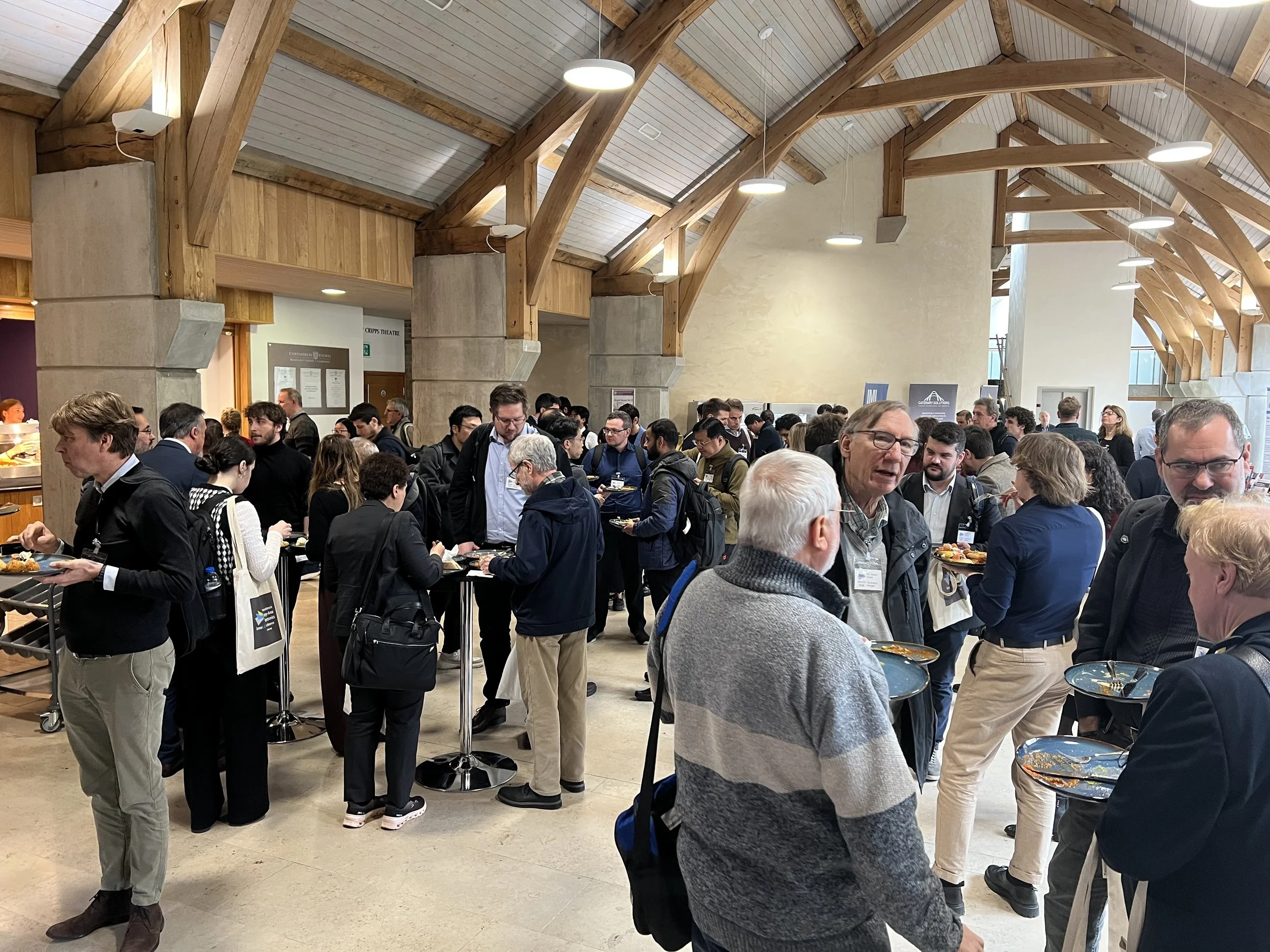
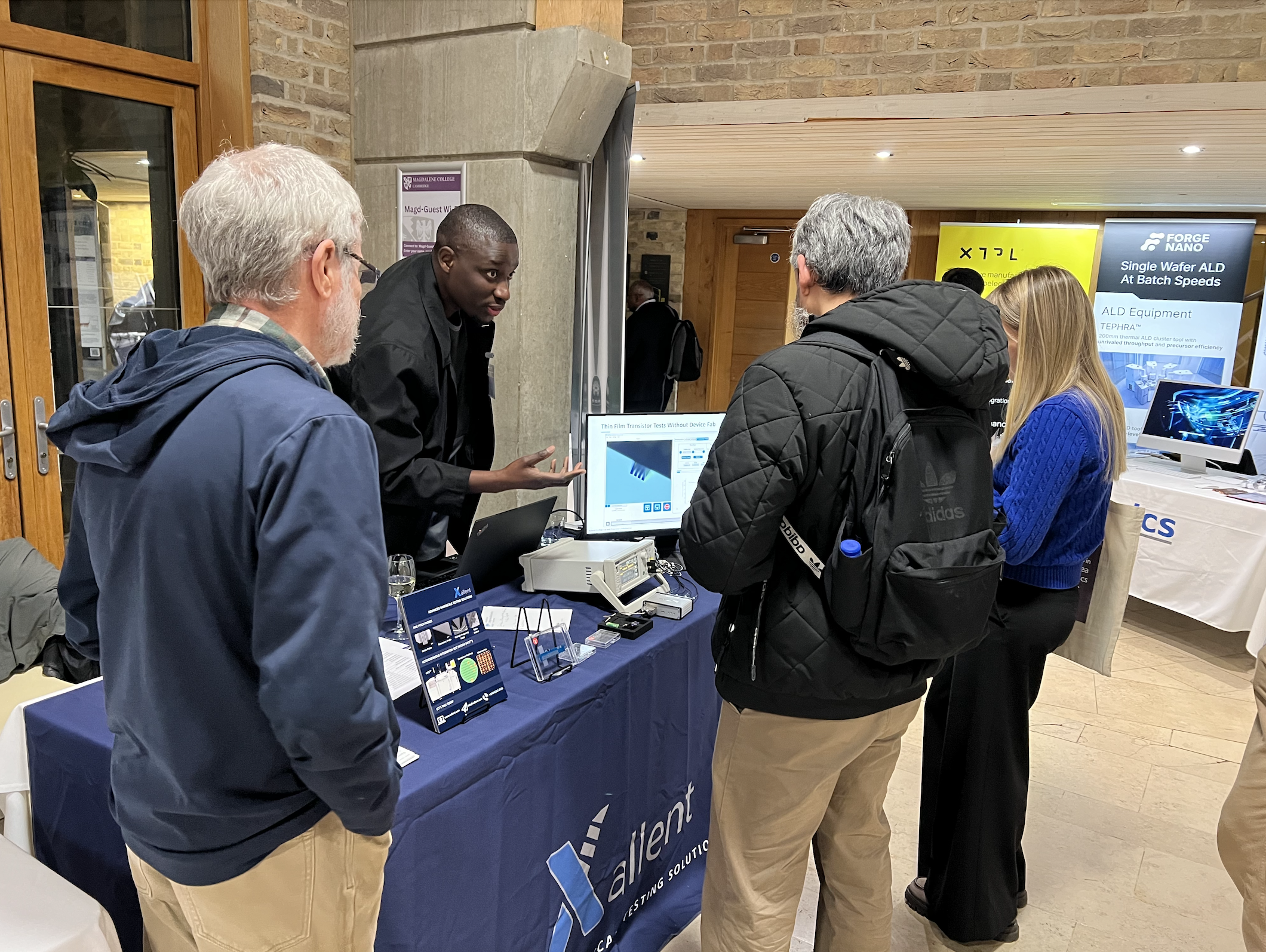
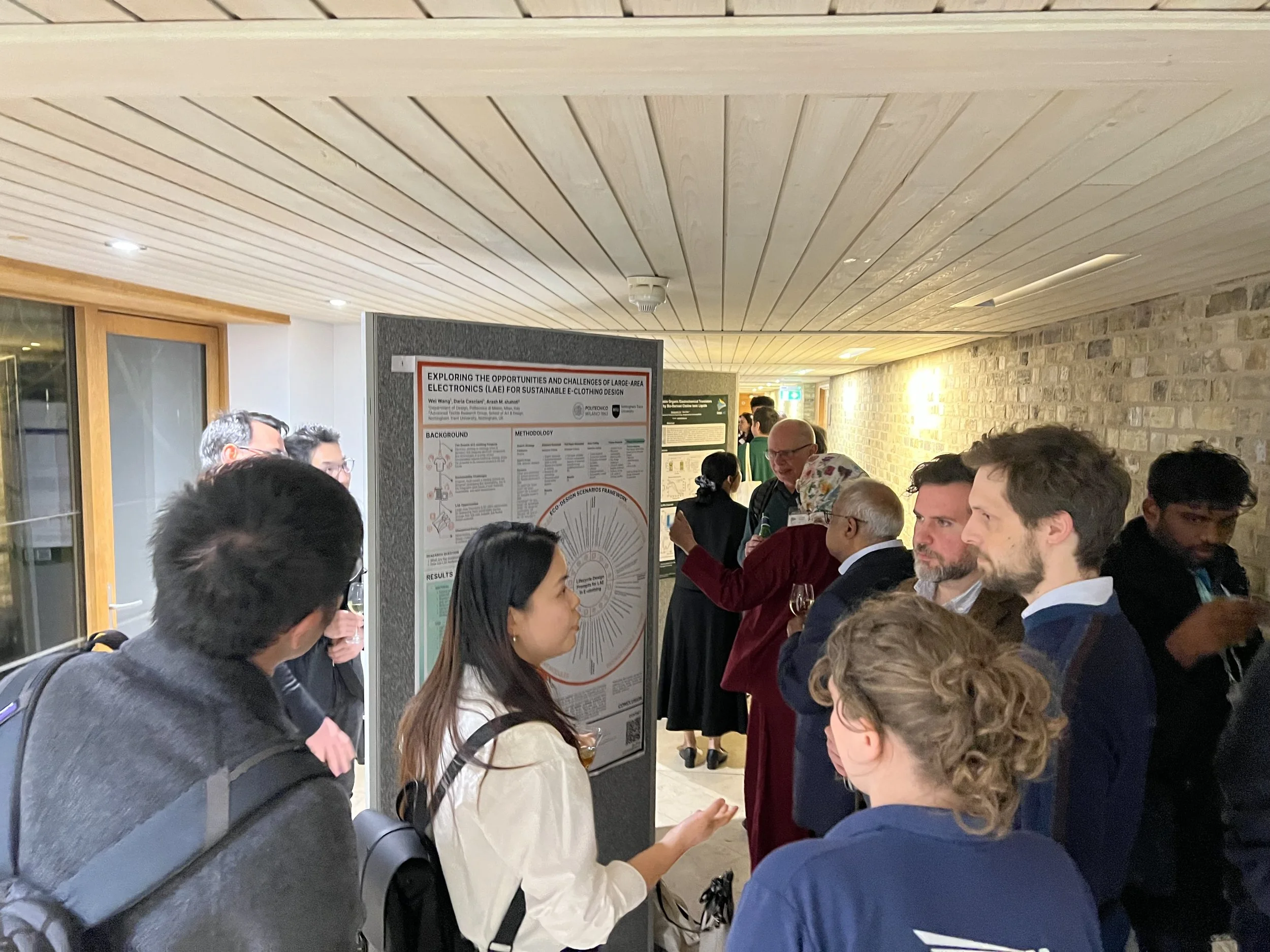
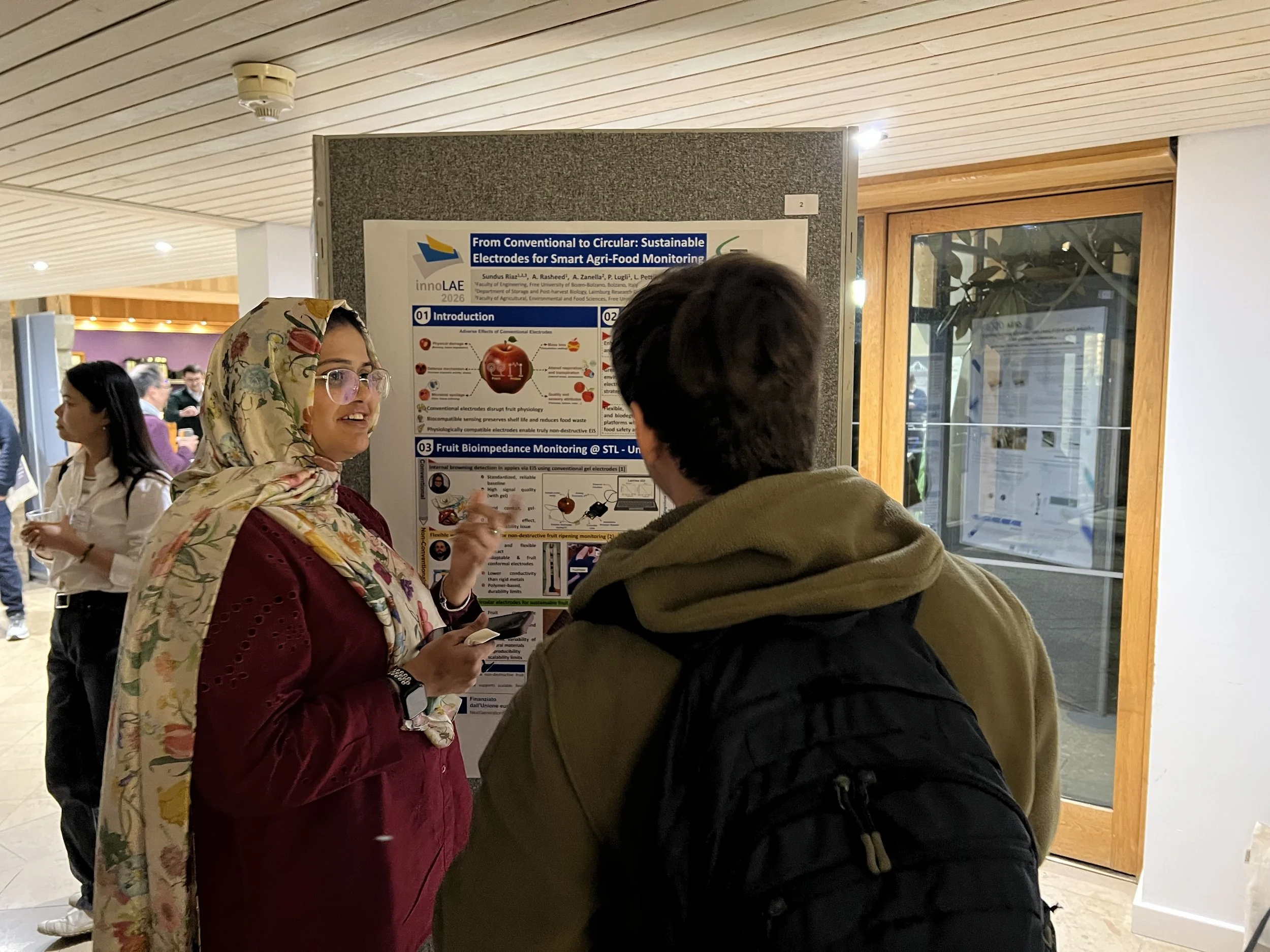
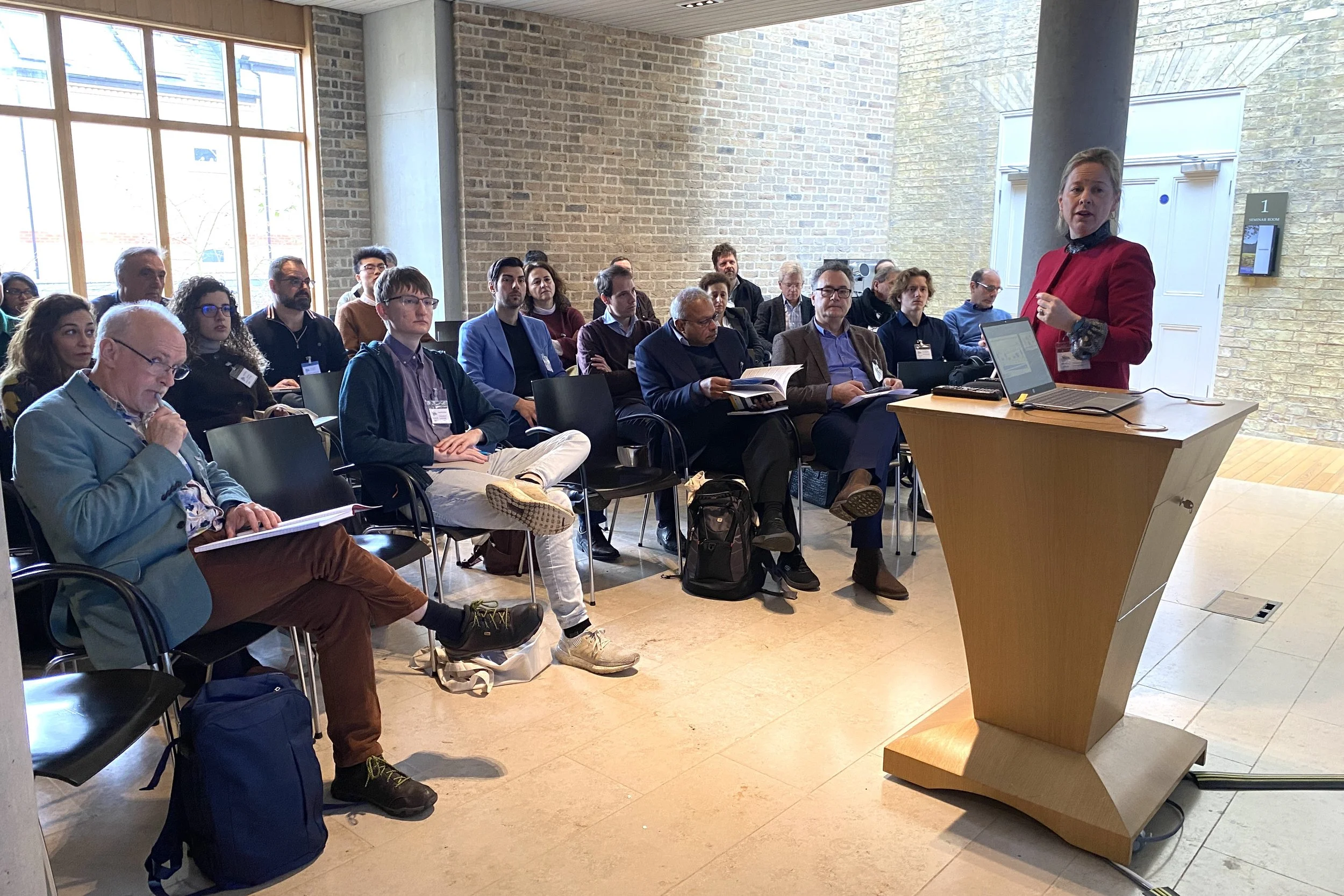
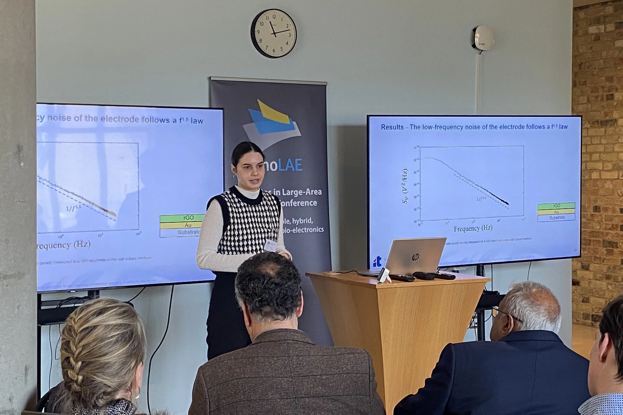
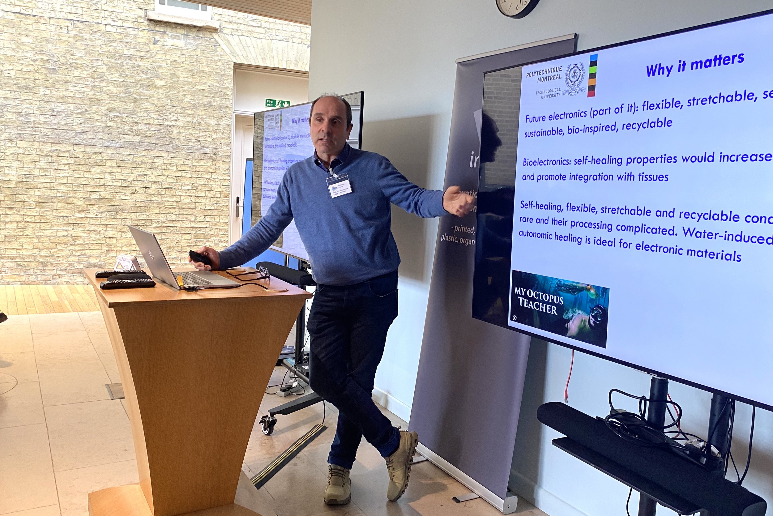
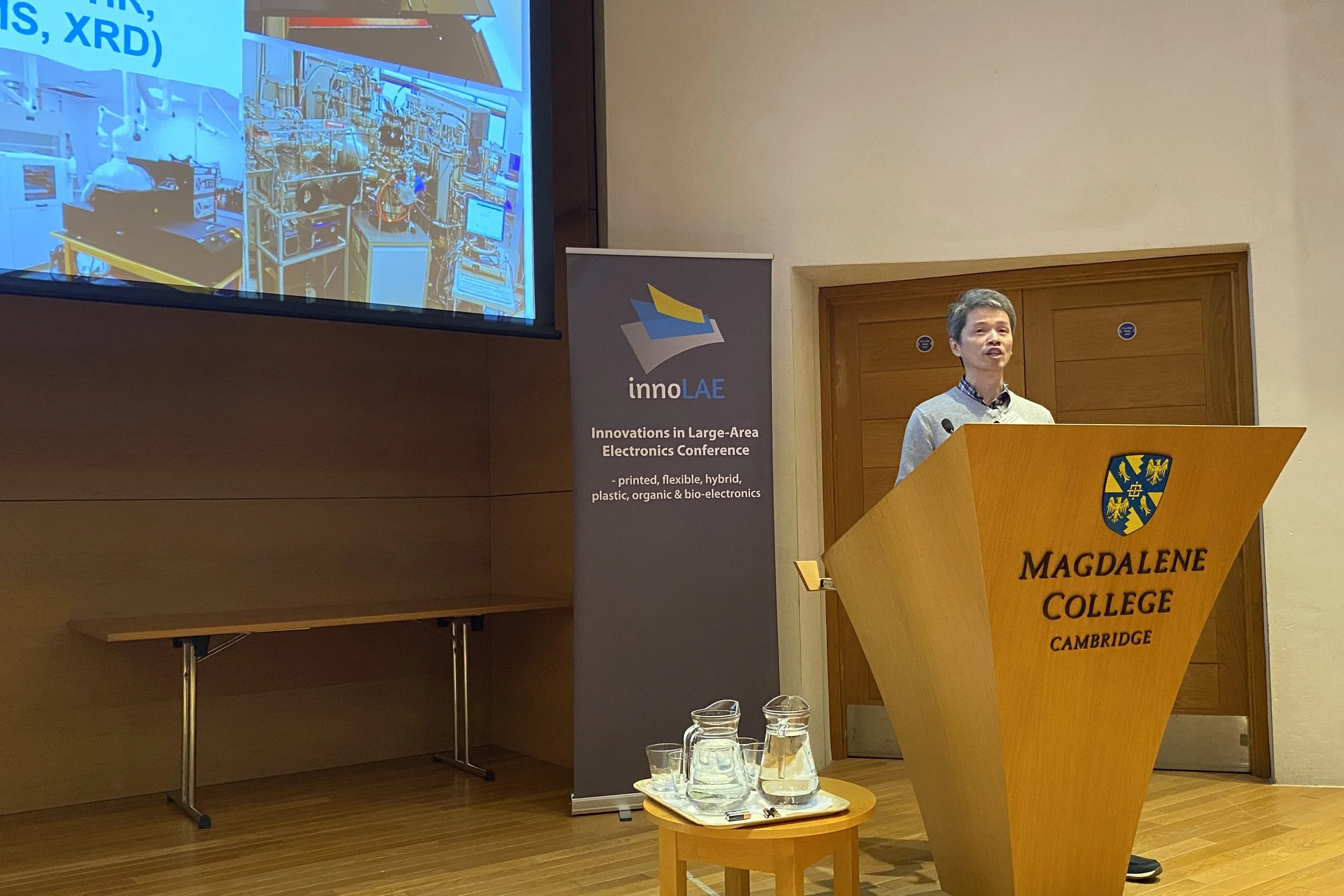
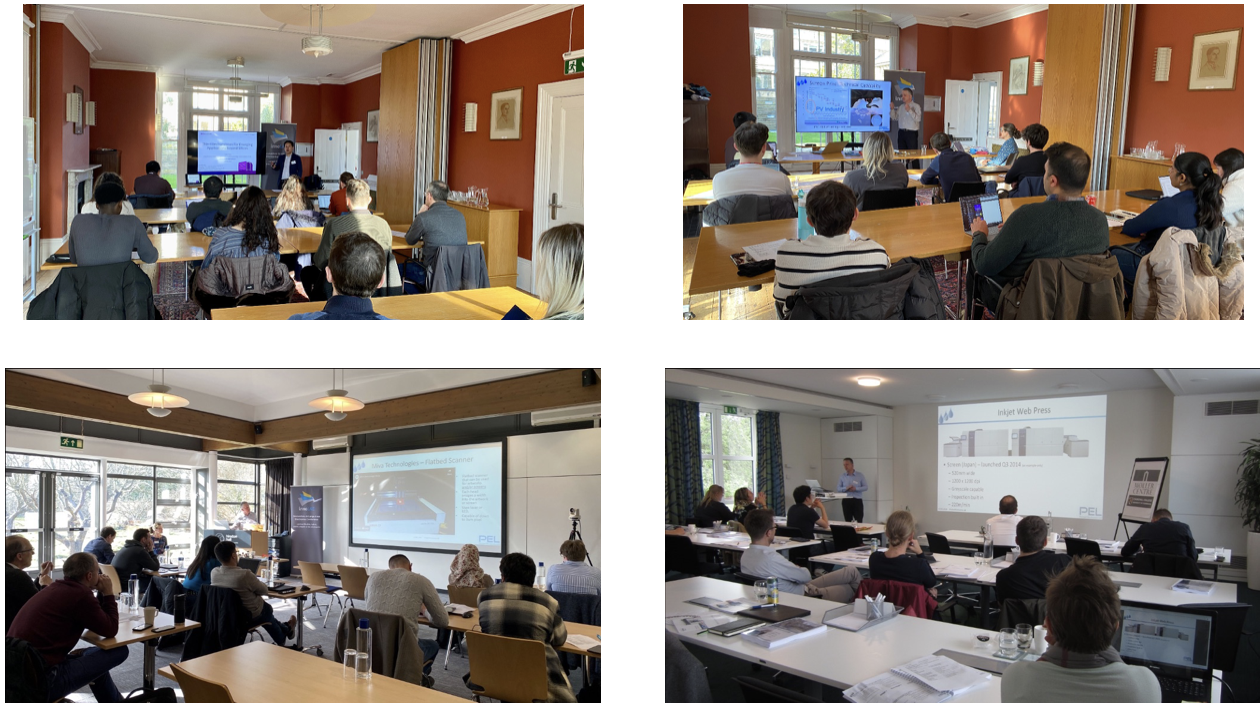
On Mon 16 – Tue 17 February, the days before the main conference, we are running a programme of technical short courses covering key topics. This is a great chance to take an in-depth look at a particular area of technology.